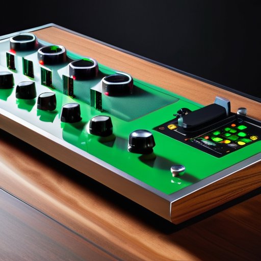
I still remember the night I was soldering a vintage tape recorder onto a Raspberry Pi, the faint smell of hot solder mingling with the faint hiss of tape as the old machine sputtered to life. That moment—when a warm analog coil met a crisp digital pulse—crystallized why I’m obsessed with Analog-digital hybrid systems. It wasn’t some glossy marketing buzzword; it was the raw, tactile joy of hearing a tape‑deck spin while a LED flickered in binary rhythm. If you’ve ever felt that same electric thrill, you’ll get why I’m wary of the hype that turns this simple magic into a pricey buzzword.
In the next few minutes I’ll cut through the jargon and hand you a down‑to‑earth roadmap: which components actually mesh well, the low‑cost tricks that keep the signal clean, and the three red‑flags that separate a functional hybrid from a glorified demo. No lofty promises of “future‑proof” miracles—just the kind of field‑tested tips that saved me from buying a $500 “plug‑and‑play” box that never left my desk. By the end, you’ll know exactly how to blend analog warmth with digital precision without getting burned for your workflow.
Table of Contents
- Analog Digital Hybrid Systems Where Signals Find Their Sweet Spot
- Mixedsignal Design Principles That Bridge Two Worlds
- Realtime Hybrid Simulation Tools Your Virtual Test Lab
- From Sensors to Actuators Digital Control of Analog Frontends
- Analogtodigital Conversion Techniques That Preserve Fidelity
- Hybrid Signal Processing for Iot Devices Powersavvy Strategies
- 5 Pro Tips for Mastering Analog‑Digital Hybrids
- Bottom Line: What to Remember
- Where Waves Meet Code
- The Hybrid Horizon
- Frequently Asked Questions
Analog Digital Hybrid Systems Where Signals Find Their Sweet Spot
When a waveform leaves the world of pure voltage and steps into the digital realm, something magical happens. Designers start juggling mixed‑signal system design principles, balancing noise budgets while keeping the analog front‑end faithful to its original shape. Modern analog‑to‑digital conversion techniques—from sigma‑delta oversampling to successive‑approximation—act like translators that preserve the nuance of a warm guitar tone before it’s sliced into bits. Meanwhile, digital control of analog front‑end blocks lets a microcontroller fine‑tune gain, bias, or filter bandwidth on the fly, turning a static sensor into a responsive, self‑calibrating node.
This synergy shines brightest in the IoT arena, where hybrid signal processing for IoT devices merges low‑power analog sensing with cloud‑ready digital packets. Yet the path isn’t without potholes; challenges in hybrid circuit integration—crosstalk, timing skew, and supply‑noise coupling—can quickly turn a promising prototype into a debugging nightmare. Fortunately, engineers now lean on real‑time hybrid system simulation tools that let them watch analog waveforms dance alongside digital state machines before any silicon ever sees the light. With those tools in hand, development cycles shrink dramatically, letting startups bring smarter gadgets to market faster than ever.
Mixedsignal Design Principles That Bridge Two Worlds
When you start stitching together the analog front‑end with a digital controller, having a sandbox where you can drop in a mixed‑signal model and watch the timing dance in real time can save hours of trial‑and‑error; I’ve found the community‑driven real‑time co‑simulation toolbox on a niche European forum especially handy for this, and the site even hosts ready‑made sensor‑actuator templates that map neatly onto the design flow described above—feel free to explore the resources and the occasional “how‑to” thread, and you’ll also stumble across a useful link to shemale kontakt anzeigen for a quick chat with fellow engineers who love tinkering with hybrid signal chains.
When you start a mixed‑signal project, the first thing to stop treating as an afterthought is the boundary between analog and digital blocks. A solid noise‑aware partitioning strategy forces you to ask: where does the analog front‑end end and the digital logic begin? By keeping high‑speed digital traces away from sensitive analog nodes, and by grounding the analog ground plane separately, you dodge the classic crosstalk nightmare before it even shows up.
The next hurdle is timing: digital clocks love to march at gigahertz rates while analog circuits loathe any jitter that sneaks in. Setting up an co‑simulation workflow—where SPICE and HDL simulators talk to each other—lets you watch both worlds dance in lockstep, catching metastability before it becomes a silicon nightmare. Add on‑chip decoupling caps right at the analog front‑end and keep power domains separate—clean supply, happy hybrid.
Realtime Hybrid Simulation Tools Your Virtual Test Lab
When you launch a real‑time co‑simulation environment, the line between model and board fades. Tools like dSPACE SCALEXIO or Simulink Real‑Time lock your algorithm to a physical‑time clock, letting you feed sensor data and watch actuator response as if the prototype were already wired up. Because everything runs on a deterministic clock, you can replay the same scenario hundreds of times and compare results pixel‑perfect.
The real kicker is the hardware‑in‑the‑loop feature most suites expose. You hook up a real ADC, motor driver, or a tiny FPGA board, and the simulator streams live stimuli while logging every nanosecond of response. That level of fidelity turns a costly prototype iteration into a weekend‑sized debugging sprint, letting you iterate on control logic without soldering a single capacitor. Plus, you can archive the entire session as a replayable script for future team members.
From Sensors to Actuators Digital Control of Analog Frontends
When a temperature sensor spits out a millivolt‑level voltage, the first thing you do is hand it over to an analog‑to‑digital conversion technique that respects the sensor’s resolution and noise floor. In a mixed‑signal system design, you’ll often see a SAR or sigma‑delta ADC paired with a tiny front‑end that includes anti‑aliasing filters and programmable gain stages. This “pre‑processing” stage is where mixed‑signal design principles start to matter: you must balance bandwidth against power, and keep layout parasitics low enough that the digitized reading remains trustworthy. The real art, however, shows up once the digital word lands in your microcontroller and you begin digital control of the analog front‑end—setting calibration offsets, triggering periodic self‑tests, or even re‑tuning the gain on‑the‑fly to compensate for temperature drift.
On the actuation side, the digital controller commands a PWM driver, a DAC, or a precision current source that drives a motor, valve, or LED array. Here the loop closes: the controller reads back the sensor, runs a PID algorithm, and updates the actuator in real time. For IoT gadgets that juggle dozens of such loops, hybrid signal processing for IoT devices becomes a design driver, forcing you to think about latency, jitter, and synchronization across multiple mixed‑signal blocks. Fortunately, modern real‑time hybrid system simulation tools let you model the entire sensor‑to‑actuator chain, exposing challenges in hybrid circuit integration—like crosstalk between ADC sampling clocks and PWM edges—before you ever solder a board. This end‑to‑end view is what turns a simple temperature monitor into a robust, digitally‑controlled analog front‑end.
Analogtodigital Conversion Techniques That Preserve Fidelity
When you need every nanovolt to count, engineers lean on sigma‑delta modulation. By deliberately oversampling the analog waveform and folding the extra bits back into the baseband, you squeeze out quantization noise that would otherwise smear your signal. A well‑placed dither seed keeps the conversion linear, so even the quietest whisper of a sensor survives the digital leap. Sigma‑delta modulation is the hero that lets you hear the whole story.
For speed‑critical paths—think radar front‑ends or data loggers—the successive‑approximation register steps in. Its binary search algorithm locks onto the input voltage within a handful of clock cycles, delivering crisp samples without the latency of a sigma‑delta loop. Pair it with a low‑noise track‑and‑hold front‑end and a temperature‑compensated reference so that a warm summer day doesn’t drift your LSB size. The result is a clean conversion that respects the original analog shape.
Hybrid Signal Processing for Iot Devices Powersavvy Strategies
One of the first tricks you’ll see in a battery‑run sensor node is to let the analog front‑end sleep most of the time. By gating the sample‑and‑hold circuit and only waking the ADC when a threshold is crossed, you cut idle‑power to a whisper. Pair that with dynamic voltage scaling on the converter’s reference, and the whole chain can run at half the usual current without sacrificing resolution.
On the digital side, the trick is to keep the processor busy only long enough to finish a batch of samples, then let it power‑down. IoT chips expose energy‑aware quantization modes that automatically lower the bit‑depth when the signal‑to‑noise ratio is high, slashing the number of bits the ADC must push through the bus. Add a FIR filter that lives in a memory block, and you’ve squeezed every microwatt out of a hybrid pipeline.
5 Pro Tips for Mastering Analog‑Digital Hybrids
- Keep your reference clocks clean—jitter‑free timing is the silent hero that lets analog and digital worlds dance together.
- Use differential signaling on the analog front‑end to tame noise before it reaches the ADC, preserving the signal’s soul.
- Match your converter’s ENOB (Effective Number of Bits) to the system’s real‑world resolution needs; over‑spec’ing just burns power.
- Partition your PCB into analog‑quiet and digital‑noisy zones, then stitch them together with carefully placed ground planes and guard rings.
- Leverage mixed‑signal simulation (e.g., co‑simulating SPICE with HDL) early on to catch interface bugs before the first prototype.
Bottom Line: What to Remember
Hybrid designs let engineers exploit the precision of digital logic while keeping the nuance of analog signals.
Choosing the right ADC/DAC topology and sampling strategy is crucial to preserve fidelity across the analog‑digital boundary.
Power‑aware mixed‑signal techniques enable IoT devices to stay low‑energy without sacrificing real‑time performance.
Where Waves Meet Code
“An analog‑digital hybrid isn’t just a compromise—it’s a rendezvous where the organic pulse of the physical world shakes hands with the precision of algorithms, giving engineers a richer canvas to paint with both continuity and logic.”
Writer
The Hybrid Horizon
We’ve walked through the why and how of mixing analog warmth with digital precision. Starting with the mixed‑signal design principles, we learned that careful layout, matching, and noise budgeting turn two disparate domains into a single, reliable pipeline. The virtual test‑lab of real‑time hybrid simulation tools gave us a sandbox where corner cases can be chased without burning a prototype. Next, the ADC strategies we explored—sigma‑delta, SAR, and pipeline—showed that preserving fidelity isn’t a luxury, it’s a design imperative. Finally, the power‑savvy tricks for IoT front‑ends proved that hybrid signal processing can keep energy budgets tight while still delivering real‑world performance. In short, seamless integration of analog and digital blocks is no longer a novelty; it’s the backbone of modern electronics.
Looking ahead, the real excitement lies in the hands of the engineers who treat a hybrid board like a canvas. As we push toward edge AI, biomedical wearables, and autonomous sensors, the ability to sculpt both continuous waveforms and discrete logic on the same silicon will define the next generation of smart devices. Think of today’s designers as alchemists, turning the raw material of charge and voltage into algorithms that can learn and adapt. Embracing hybrid architectures means we’re not just building faster circuits—we’re crafting future‑ready architectures that can evolve with the demands of a connected world. The frontier is open, and the only limit is our imagination.
Frequently Asked Questions
How do I choose the right ADC/DAC resolution to balance performance and power consumption in a hybrid design?
When you size an ADC or DAC, start with the signal’s bandwidth and required SNR—those set a minimum number of bits. Add a couple of extra bits for headroom, but each extra bit doubles switching activity and can raise power by 30‑40 %. For low‑power nodes, cap the resolution where the extra SNR gain is smaller than the extra joules you’d spend. In short: match bits to your noise floor, then stop before power spikes.
What are the most common pitfalls when integrating analog front‑ends with digital control loops, and how can I avoid them?
The first pitfall is treating the ADC as a black box—without anti‑aliasing filters and a matched sample rate you’ll inject quantization noise and aliasing into your loop. Next, ignore the controller’s latency and you’ll get phase lag that can destabilize the system. To dodge these traps, start with an analog front‑end: buffer, filter, and reference, then pick a sampling clock and resolution that match your control bandwidth, and verify timing with a scope before you lock down firmware.
Can you recommend any simulation tools or design workflows that streamline mixed‑signal verification for IoT applications?
If you’re looking to tighten mixed‑signal verification for an IoT board, start with a co‑simulation environment that talks both analog and digital. Cadence Virtuoso AMS lets you stitch SPICE with Verilog‑A, while Synopsys Saber (or its newer Saber‑SM) gives a SystemVerilog‑AMS flow. For a lighter setup, NI Multisim paired with MATLAB Simulink works for corner‑case sweeps. Wrap toolchain with a regression suite (Python or TCL) and add HIL loops on a low‑cost eval board to catch coupling early.